The RP2040 as a SNES sound chip, at 97 per cent of realtime
The from-scratch SNES core is still over its cycle budget on the H7. In the last post I measured where every millisecond goes, and one pool stood out: the APU. The SNES sound system is a whole second computer, an SPC700 CPU plus an 8-voice DSP with its own 64KiB of RAM, and emulating it costs the H7 a measured 3.32 million cycles per frame. That is 12.4% of the entire frame budget spent on a chip whose only connection to the main CPU is four byte-wide ports.
Four bytes of seam. And sitting right there on the board, already driving the HDMI output, is an Adafruit Feather RP2040 DVI with one core mostly idle.
The real SNES solved this problem with separate silicon. The question practically asks itself: can the Feather be the sound chip?
Two wires
The existing link to the Feather is one-way by design: the H7 streams pixels over SPI and nothing ever comes back. A sound chip needs to answer (the boot handshake is bidirectional), so the first job was hardware: a return data wire and a ready line.
The Feather end was easy, two free GPIOs. The Nucleo end took an evening with the board manual, because the useful pins had to terminate somewhere a soldering iron can actually reach: the morpho prototyping holes beside the Zio headers. GP24 became a 2MBaud UART into PF6 at morpho hole CN11-9, and GP25 became a ready interrupt into PA15 at CN11-17. PA15 is the JTAG TDI pin, which is fine under SWD but boots with a pull-up, so the firmware has to treat a high line as meaningless until the far end claims it.
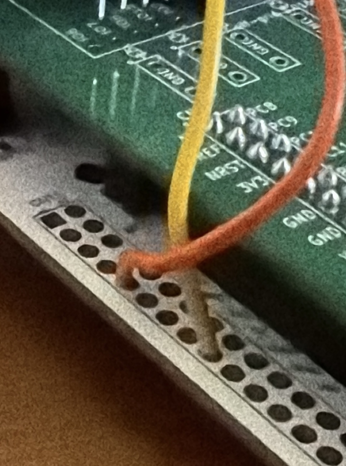
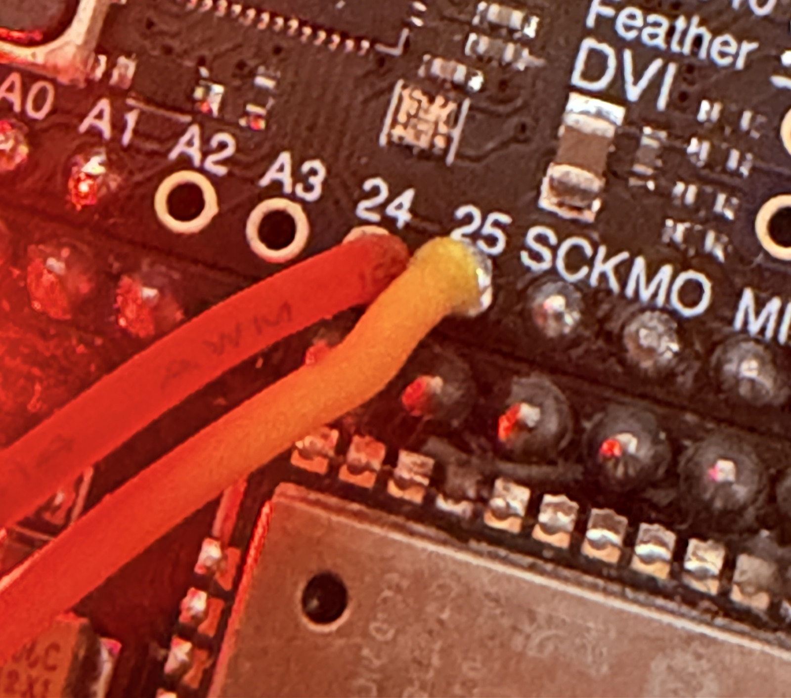
The first link test failed completely. Every ping timed out, hundreds per second, while the DVI colour bars sat there smugly proving the board was alive. I stared at the wiring photos for a while before cross-checking the one thing I had not: the SPI mode. My own production sender carries a comment I wrote weeks ago saying the RP2040's PL022 is unreliable as an SPI slave with CPHA=0. The probe was using CPHA=0. One line later:
paced ok=893/s rtt us min=115 avg=116 max=122 ready-gap us avg=87 crc=0 seq=0 timeout=0
burst ok=8457/s rtt us min=116 avg=116 max=117 crc=0 seq=0 timeout=0
8,457 round trips per second, sustained, with under 2us of jitter and not a single CRC error, while HDMI kept scanning. The wires were never the problem. The wires are never the problem until they are, which is why you prove them first.
Stealing a sound track from determinism
Testing a sound chip needs music. Real music, not a synthetic loop, because the expensive parts of the DSP (gaussian interpolation, echo, eight envelopes) only light up when a real driver plays real samples.
Here the SPC700 hands you a gift: it is fully deterministic from reset. Its only input is those four ports. If I record every port write the game makes, with the exact APU cycle each one lands on, then replaying those writes at those cycles reproduces everything: the boot handshake, the sound driver upload, and the music. No game, no CPU, no cartridge needed on the other end.
So the emulator core grew a one-line tap on its APU write path, and the 750-frame Super Mario World test run I already use for correctness produced a trace:
/// Observer for every APU port write, timestamped after catch-up.
pub apu_port_tap: Option<fn(u64, u8, u8)>,
94,288 port writes over 750 frames. The busiest frame is frame 17 with 1,366 writes, which is the driver upload burst right after power-on. And the crucial check: with the tap installed, the run still produces the exact final frame hash it always has. Observation without perturbation.
The replay end mirrors the emulator's own catch-up semantics: run the SPC to each write's cycle boundary, land the write, keep going. After the last event the uploaded driver just keeps playing its level theme forever, which makes it the perfect sustained workload. The best part is what happened on screen later: the trace ends, and the port bytes keep cycling through the driver's handshake values on their own. The little computer is alive and playing music to nobody.
A sound chip with no framebuffer
The bench firmware puts LakeSnes's SPC700 and DSP on core 0 of the RP2040 - the exact code my own emulator uses both as its correctness oracle and, today, as its actual sound chip behind the four-byte seam - while core 1 keeps generating DVI with PicoDVI. There is no framebuffer at all: every scanline is generated procedurally, colour bars plus two status stripes, so all the RAM belongs to the APU. A white bar grows with trace progress; a magenta block sweeps the screen driven by the APU cycle counter. If the APU stalls the block freezes while the bars keep scanning. If DVI dies, everything freezes. Diagnosis by eyeball.
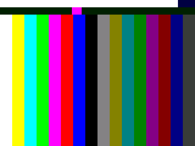
Re-render of the bench screen, not a capture: the white trace-progress stripe, the sweeping magenta APU marker, and the bars.
One memory trick worth recording: LakeSnes's APU carries a pointer to the whole console struct, which is 131KiB, half the chip's RAM. But it only ever dereferences it inside one sync function I never call, because the bench drives the SPC directly. So the carrier pointer is NULL and the sound chip fits in about 76KiB of heap.
The measurement ladder, including the rungs I fell through
First flash: the screen went solid red and the telemetry came back reading like a broken clock:
t=6s apu_cyc=6843627 (667% rt) busy=13167942us (1316%) chunk_max=13167942us dvi_fps=285Thirteen seconds of busy time in a one-second window. The pacing loop chased a fixed target, but the emulation ran slower than realtime, so every chase took longer than the deficit it started with and the report window doubled each pass. Once I bounded the chase into 50ms slices the real number emerged: 0.50x realtime, with DVI starved below 30fps. The SPC700 was executing from XIP flash, and two cores fighting over one QSPI bus is a fight everybody loses.
The fix is my favourite kind: the Pico SDK's linker script already has an escape hatch for exactly this, a list of files whose code gets copied to SRAM at boot. Three additions:
*(EXCLUDE_FILE(*libgcc.a: *libc.a:*lib_a-mem*.o *libm.a: *apu.c.o *spc.c.o *dsp.c.o) .text*)42.6KiB of sound chip moved into RAM. Result: 0.67x. Better, still failing, and DVI was still stuck under 50fps, which I confidently blamed on bus contention between the cores.
Then I measured the baseline properly: five seconds of scanout with core 0 completely idle came back at 49fps. There was no contention. My own bar renderer was computing a division per pixel, and the M0+ turns every one of those into a library call. The MD receiver I based this on uses palette lookups precisely to avoid this, and I had walked straight past the lesson. Prebuilt rows and span fills later: 60fps baseline, and 60fps under full APU load too. The contention theory died on that number, which is exactly what baselines are for.
From there it was a clean clock ladder. PicoDVI ties the system clock to the DVI bit clock, so more CPU speed means changing display mode:
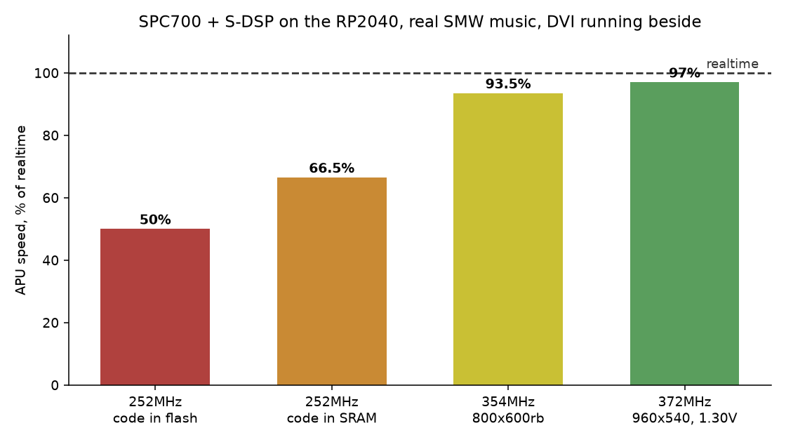
354MHz scales the 0.665 to 0.935, which is linear to three digits: this workload is purely compute-bound. The last step, 372MHz with the 960x540 mode, produced the day's best plot twist. At the vendor's suggested 1.25V the APU finally cleared realtime, 103%, while the screen went black: the scanout core had wedged within three seconds. Slower silicon needs 1.30V at that clock, the documentation says so, and at 1.30V both cores ran all day: DVI rock solid at 60fps, and the APU at
97% of realtime.
Three percent short. With the music playing, the deficit grows by about 22ms every second, forever.
Why 97% is the most valuable number
A guessed 100% would have told me nothing. This 97% tells me almost everything:
- The scaling is linear across a 1.5x clock range, so this is a real compute limit, not a cache effect or a bus accident I could tune away.
- It is an upper bound. The bench does no PCM output, no link receive, no control traffic. Real duty only subtracts.
- 372MHz at 1.30V is the end of the road: the system clock is chained to the DVI bit clock and there is no faster DVI-compatible operating point on this part.
- And the architecture around the number works: bidirectional transport at 116us round trips, a full SPC700+DSP and 60fps HDMI sharing one 264KiB microcontroller without dropping either.
So the decision writes itself. I am not splitting the SPC and DSP across the two cores: they share that 64KiB of audio RAM sample by sample, and the coherence design would become the whole project in exchange for three percent. I am not optimising the reference core first either; needing ten percent from mature code is the kind of plan that eats a month and returns four. The H7 still has bigger, better-understood pools to attack, so the main perf arc resumes there.
But the coprocessor architecture stays. Every piece of it is now proven hardware fact rather than diagram: the protocol, the return channel, the replay bench, the failure modes. And the RP2350 exists, with an HSTX peripheral that unties the system clock from the video clock entirely. When a revision 2 board happens, the sound chip experiment is already de-risked. The two bodge wires bought that.
The screen is back to sixteen bars of another kind now: the product bridge is reflashed, the console shell is on HDMI, and somewhere in a log file there is a record of an RP2040 spending its afternoon as a Super Nintendo sound chip, three percent too slowly, and proving exactly where the limit is.